- 您现在的位置:买卖IC网 > Sheet目录1193 > AD8231-EVALZ (Analog Devices Inc)BOARD EVAL FOR AD8231
�� �������
�������Zero� Drift,� Digitally� Programmable�
�I� nstrumentation Amplifier Evaluation� Board�
�AD8231-EVALZ�
�FEATURES�
�Two� AD8231� circuits�
�In-amp� and� op� amp�
�Differential� output�
�Easy� to� switch� jumpers�
�QUICK� START�
�Set� the� jumpers� as� shown� in� Table� 1.� These� jumper� settings� ensure�
�the� part� is� enabled� and� in� a� gain� of� 1.�
�Table� 1.� Quick� Start� Jumper� Settings�
�Decoupled� supply� lines�
�GENERAL� DESCRIPTION�
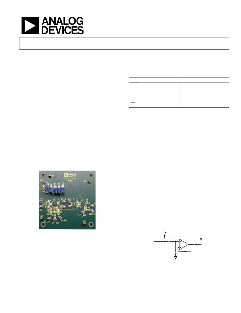
�The� AD8231-EVALZ� has� two� AD8231s� mounted� on� it.� Z1� is� the�
�AD8231� on� the� left� side� of� the� board.� It� is� configured� to� allow�
�access� of� the� in-amp� and� op� amp� separately.� Z2� is� the� AD8231�
�Function�
�SDN�
�A2�
�A1�
�A0�
�CS�
�Setting�
�High�
�Low�
�Low�
�Low�
�Low�
�on� the� right� side� of� the� board.� It� is� set� up� as� a� differential� output�
�configuration.�
�Inputs,� outputs,� references,� and� the� supplies� are� routed� to� test�
�points� for� easy� connectivity.� SDN,� CS,� and� the� gain� select� pins�
�(A0� to� A2)� are� routed� to� jumpers.� These� jumpers� control� both�
�AD8231s.� When� a� jumper� is� in� the� high� position,� its� corresponding�
�pin� is� connected� to� VS.� When� the� jumper� is� in� the� low� position,�
�it� is� connected� to� ground.�
�The� PCB� has� four� layers.� The� top� and� bottom� layers� are� used� for�
�routing,� and� the� two� internal� layers� are� power� and� ground� planes.�
�EVALUATION� BOARD�
�Connect� the� ground� lead� to� GND� and� connect� a� 5� V� supply� to�
�+V� S.� Connect� a� 1� V� source� to� –INA,� and� connect� a� 2� V� source� to�
�+INA.� 3.5� V� should� now� appear� at� OUTA.�
�The� output� equation� for� the� AD8231� with� a� gain� of� 1� is�
�V� +INA� ?� V� ?INA� +� V� REF� =� V� OUT� .� As� shipped,� the� evaluation� board�
�has� the� in-amp� reference� pin� driven� to� half� the� supply� voltage.�
�Therefore,� the� output� voltage� is� 2� V� –� 1� V� +� 2.5� V� =� 3.5� V.�
�DUAL� SUPPLIES�
�The� supplies� on� the� AD8231-EVALZ� are� labeled� VS� and� GND�
�because� most� applications� are� single� supply.� However,� dual�
�supplies� can� also� be� used� with� this� evaluation� board,� as� long� as�
�the� difference� between� the� two� supplies� is� less� than� 6� V.� Simply�
�connect� the� negative� supply� to� the� GND� terminal.� For� example,�
�connect� +2.5� V� to� +V� S� and� ?2.5� V� to� GND.� Any� voltage� connected�
�to� GND� also� appears� at� the� GND1,� GND2,� and� GND3� terminals;�
�therefore,� take� care� when� connecting� external� equipment.�
�CONFIGURING� THE� OP� AMP�
�By� default,� the� op� amp� in� Z1� is� configured� as� a� unity-gain� buffer�
�driving� the� in-amp� reference� pin.� A� resistor� divider� at� the� op� amp�
�input� sets� the� voltage� at� midsupply.� When� using� this� op� amp� for�
�other� applications,� remove� R8� and� drive� the� in-amp� REF� pin�
�with� a� different� source.�
�VS�
�Figure� 1.�
�OP_IN�
�R10�
�0� ?�
�R7�
�10k� ?�
�R13�
�0� ?�
�R8�
�0� ?�
�OP_OUT�
�REF�
�RC11�
�10k� ?�
�R12�
�0� ?�
�Figure� 2.� Default� Op� Amp� Configuration�
�Rev.� 0�
�Evaluation� boards� are� only� intended� for� device� evaluation� and� not� for� production� purposes.�
�Evaluation� boards� are� supplied� “as� is”� and� without� warranties� of� any� kind,� express,� implied,� or�
�statutory� including,� but� not� limited� to,� any� implied� warranty� of� merchantability� or� fitness� for� a�
�particular� purpose.� No� license� is� granted� by� implication� or� otherwise� under� any� patents� or� other�
�intellectual� property� by� application� or� use� of� evaluation� boards.� Information� furnished� by� Analog�
�Devices� is� believed� to� be� accurate� and� reliable.� However,� no� responsibility� is� assumed� by� Analog�
�Devices� for� its� use,� nor� for� any� infringements� of� patents� or� other� rights� of� third� parties� that� may� result�
�from� its� use.� Analog� Devices� reserves� the� right� to� change� devices� or� specifications� at� any� time�
�without� notice.� Trademarks� and� registered� trademarks� are� the� property� of� their� respective� owners.�
�Evaluation� boards� are� not� authorized� to� be� used� in� life� support� devices� or� systems.�
�One� Technology� Way,� P.O.� Box� 9106,� Norwood,� MA� 02062-9106,� U.S.A.�
�Tel:� 781.329.4700� www.analog.com�
�Fax:� 781.461.3113� ?2008� Analog� Devices,� Inc.� All� rights� reserved.�
�发布紧急采购,3分钟左右您将得到回复。
相关PDF资料
AD8348-EVALZ
BOARD EVAL FOR AD8348
AD8436-EVALZ
BOARD EVAL FOR AD8436
AD9352-5/PCBZ
EVALUATION BOARD
AD9550/PCBZ
BOARD EVALUATION FOR AD9550
AD9985A/PCBZ
KIT EVALUATION FOR AD9985A
ADA4850-2YCP-EBZ
BOARD EVAL FOR ADA4850-2YCP
ADA4899-1YCP-EBZ
BOARD EVAL FOR ADA4899-1YCP
ADA4937-1YCP-EBZ
BOARD EVAL FOR ADA4937-1YCP
相关代理商/技术参数
AD8231TCPZ-EP-R7
功能描述:IC INSTR AMP PROGR ENH 16LFCSP RoHS:是 类别:集成电路 (IC) >> Linear - Amplifiers - Instrumentation 系列:- 标准包装:150 系列:- 放大器类型:音频 电路数:2 输出类型:- 转换速率:5 V/µs 增益带宽积:12MHz -3db带宽:- 电流 - 输入偏压:100nA 电压 - 输入偏移:500µV 电流 - 电源:6mA 电流 - 输出 / 通道:50mA 电压 - 电源,单路/双路(±):4 V ~ 32 V,±2 V ~ 16 V 工作温度:-40°C ~ 85°C 安装类型:表面贴装 封装/外壳:8-TSSOP(0.173",4.40mm 宽) 供应商设备封装:8-TSSOP 包装:管件
AD8231WACPZ-RL
功能描述:IC AMP INST RRO 2.7MHZ 16LFCSP RoHS:是 类别:集成电路 (IC) >> Linear - Amplifiers - Instrumentation 系列:- 标准包装:50 系列:LinCMOS™ 放大器类型:通用 电路数:4 输出类型:- 转换速率:0.05 V/µs 增益带宽积:110kHz -3db带宽:- 电流 - 输入偏压:0.7pA 电压 - 输入偏移:210µV 电流 - 电源:57µA 电流 - 输出 / 通道:30mA 电压 - 电源,单路/双路(±):3 V ~ 16 V,±1.5 V ~ 8 V 工作温度:-40°C ~ 85°C 安装类型:表面贴装 封装/外壳:14-SOIC(0.154",3.90mm 宽) 供应商设备封装:14-SOIC 包装:管件 产品目录页面:865 (CN2011-ZH PDF) 其它名称:296-1834296-1834-5
AD8232
制造商:AD 制造商全称:Analog Devices 功能描述:Single-Lead, Heart Rate Monitor Front End
AD8232ACPZ
制造商:AD 制造商全称:Analog Devices 功能描述:Single-Lead, Heart Rate Monitor Front End
AD8232ACPZ-R7
功能描述:仪表放大器 ECG and HRM IC Single Lead RoHS:否 制造商:Texas Instruments 通道数量: 输入补偿电压:150 V 可用增益调整: 最大输入电阻:10 kOhms 共模抑制比(最小值):88 dB 工作电源电压:2.7 V to 36 V 电源电流:200 uA 最大工作温度:+ 125 C 最小工作温度:- 40 C 封装 / 箱体:MSOP-8 封装:Bulk
AD8232ACPZ-RL
功能描述:仪表放大器 ECG and HRM IC Single Lead RoHS:否 制造商:Texas Instruments 通道数量: 输入补偿电压:150 V 可用增益调整: 最大输入电阻:10 kOhms 共模抑制比(最小值):88 dB 工作电源电压:2.7 V to 36 V 电源电流:200 uA 最大工作温度:+ 125 C 最小工作温度:- 40 C 封装 / 箱体:MSOP-8 封装:Bulk
AD8232ACPZ-WP
功能描述:仪表放大器 ECG and HRM IC Single Lead RoHS:否 制造商:Texas Instruments 通道数量: 输入补偿电压:150 V 可用增益调整: 最大输入电阻:10 kOhms 共模抑制比(最小值):88 dB 工作电源电压:2.7 V to 36 V 电源电流:200 uA 最大工作温度:+ 125 C 最小工作温度:- 40 C 封装 / 箱体:MSOP-8 封装:Bulk
AD8232-EVAL
制造商:Analog Devices 功能描述:Eval. Board Heart-Rate Monitor Front End